Innovate Spotlight
Albany NanoTech Complex and Semiconductor Innovation
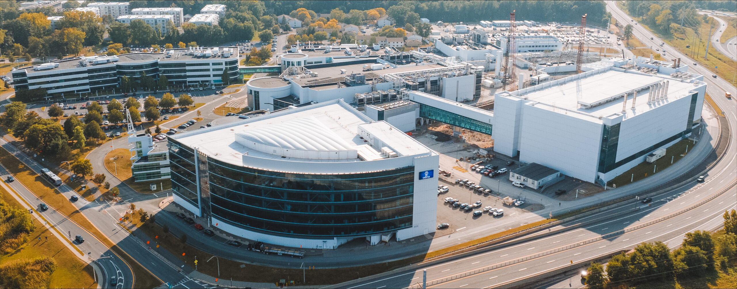
NY Creates’ Albany NanoTech Complex embodies the Empire State’s push to spur semiconductor development.
Content
Overview
What was a single building has become a hub for global semiconductor technology advancements and breakthroughs.
Back in 1997, New York State and SUNY Polytechnic Institute launched the Center for Environmental Sciences and Technology Management, a $16.5 million, 70,000-square-foot building with 4,000 square feet of cleanroom space and metrology labs for nanotechnology and semiconductor research and development.
Today, what is now the 1.65 million-square-foot Albany NanoTech Complex is also North America’s largest, most advanced semiconductor research-and-development facility of its kind, supporting about 3,000 research and development jobs. Its High-NA EUV Center will be the only U.S. location, and one of only two public R&D sites globally, with the world’s most advanced lithography technology.
Managed by NY Creates, the complex has become not just a testament to strategic planning and public-private cooperation, but also a powerful engine for semiconductor research, innovation, and economic growth containing technologies.
“By securing the most advanced chipmaking technology on the planet for NY Creates and the Albany NanoTech Complex, we are turning a promise into reality. New York State will be the preeminent hub for cutting-edge chip design for decades to come.”
— New York Gov. Kathy Hochul.
A growing center of innovation, and then a major partnership
The center’s growth surged from 2003 to 2015, adding six spaces covering 1.2 million square feet. That space included 143,825 square feet of cleanroom space, an essential element for chipmaking. The center’s NanoFab South extension houses Tokyo Electron’s Technology Center for America, which was founded in 2003 and has a 12,424-square-foot cleanroom lab.
This growth helped establish the site as the Albany NanoTech Complex. In 2018, New York State launched the nonprofit New York Center for Research, Economic Advancement, Technology, Engineering and Science, aka NY Creates, to manage and operate the complex. The move fit with the state’s broader goals to spur technological innovation and stoke economic and workforce development.
Ny Creates took over managing the Albany NanoTech Complex from its previous managers, the College of Nanoscale Science and Engineering and SUNY Polytechnic Institute.
In 2023, New York Gov. Kathy Hochul announced a $10 billion partnership with semiconductor industry leaders including Applied Materials, IBM, Micron and Tokyo Electron to establish a next-generation semiconductor research and development center at Creates’ Albany NanoTech Complex.
The major partnership, notably, would fund construction of a cutting-edge High NA Extreme Ultraviolet Lithography Center, the only such publicly owned plant, to support semiconductor research and development using the technology.
“EUV lithography has emerged as the cornerstone technology to enable the high-volume production of smaller, faster, and more efficient chips,” said Deirdre Hanford, CEO of Natcast, the National Center for the Advancement of Semiconductor Technology.
Evolving into the future
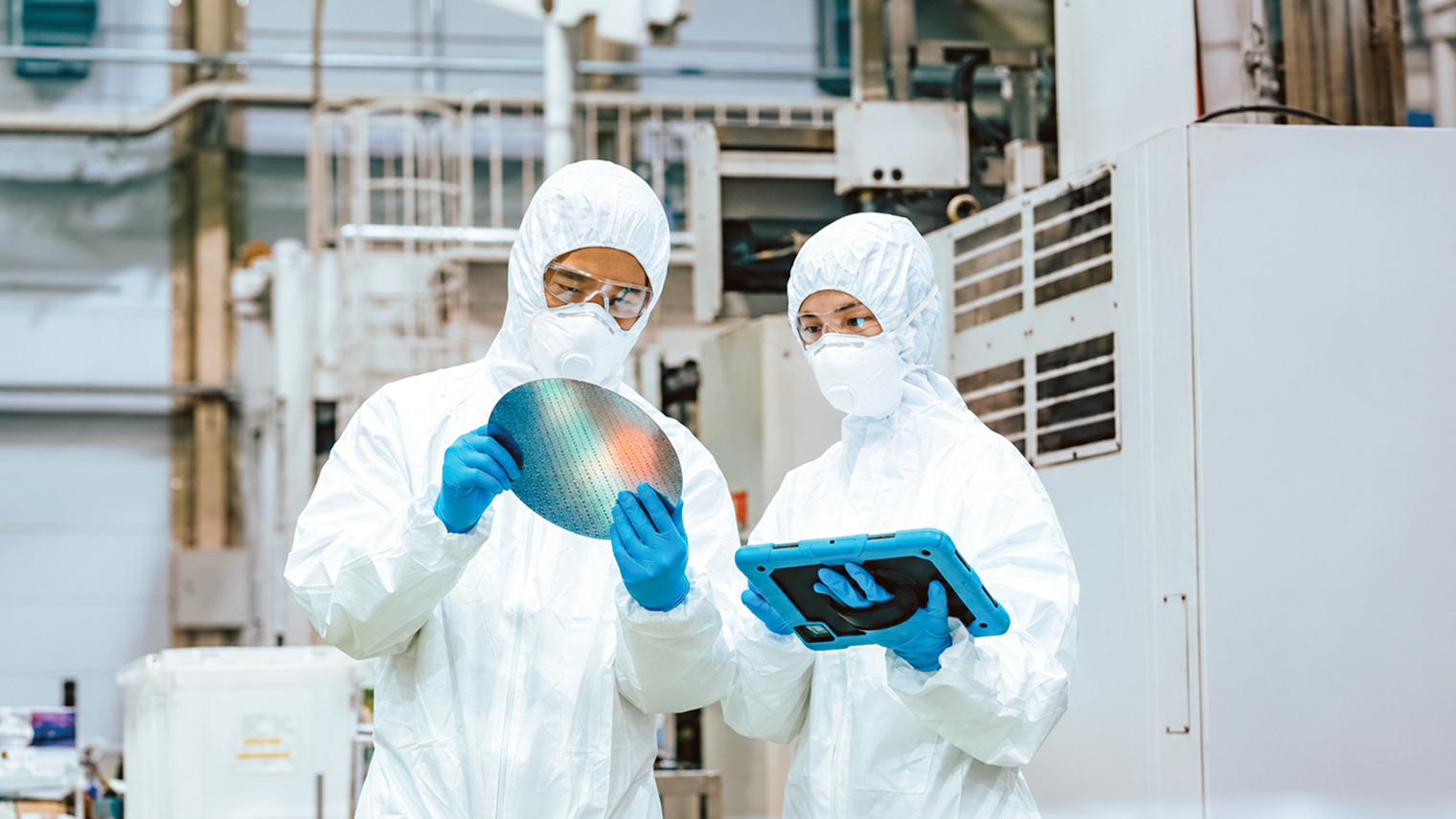
The complex continues to evolve. In December 2025, NanoFab Reflection, which will house the lithography center, saw crews install the structure’s final steel beam. A few months later, the first major piece of equipment to be delivered for the EUV Lithography Center — Tokyo Electron’s leading-edge 300mm wafer coater/developer system, CLEAN TRACK™ LITHIUS Pro DICE™ — also arrived at the Nanofab Reflection. Work on the building, which will include a 50,000-square-foot cleanroom space with temperature-controlled environments, is expected to finish by year-end 2027.
There have also been a flurry of activity and announcements at the complex in 2026:
- Screen, a Japanese semiconductor supply chain company, agreed to a 10-year, $75 million research partnership with NY Creates. Screen will also lease 10,000 square feet of space within NanoFab Reflection.
- SEMI Foundation and the federal government named NY Creates a hub for regional workforce development. The Initiative brings industry, workforce organizations, higher education institutions, and economic development partners across 12 states to train the next generation of semiconductor workforce.
- IBM announced America’s first quantum foundry, with plans to establish America’s first purpose-built quantum computing wafer foundry headquartered at the complex. Backed by $1 billion in federal CHIPS Act R&D funding and $1 billion from IBM, the initiative produces 300mm quantum-grade superconducting wafers. IBM also recently debuted the world’s first sub-1nm chip, which was made at the complex.
Learn more
From a single research building to a global hub for semiconductor and quantum innovation, the Albany NanoTech Complex reflects the power of sustained public-private investment. Its expanding facilities, partnerships and workforce programs position it to shape the next generation of U.S. technology. Learn more about the Albany NanoTech Complex here.
View all case studies